Many thanks to John VK4TJ for the excellent revision of the first section
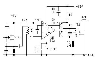
Push-pull Linear Amplifier with NE592 Driver
Transformer T1 matches the relatively low impedance present at the VFO FET gate to the balanced inputs of the NE592. With a unipolar power supply, it is necessary to bias both inputs to roughly one-half of Vcc. Below, we have shown both inputs tied to +6 VDC, conveniently available from the VFO. If 6 volts were not available, we would employ a scheme identical to the "IF amplifier" shown earlier, with Vcc split in half with 2 4,7K-ohm resistors in a divider configuration, applied to both inputs. Normally, stage gain is determined by the value of a resistor between pins 2 & 7. Bench tests reveal better output symmetry, however, if we replace this resistor with a 1 nF capacitor.
Approximately 8 volts of RF drive is available at pins 4&5 if we don't load it too heavily. This is sufficient to drive a pair of 2N3906 PNP transistors in push-pull to roughly 1,5 watts output with excellent efficiency. With bias provided by the NE592, the output transistors are operated in their linear region. Push-pull operation provides inherent suppression of even-order harmonics (2f, 4f, etc.), thereby simplifying our output network design (not shown). T2 is a T44-2 toroid with 5 bifilar primary turns and a single 5 turn secondary. C1 is around 270 pF (for 10 MHz), and should be adjusted to resonate the primary of T2 to signal frequency.
Fig 1: Schematic of the push-pull final (Pin designations are for the 8
pin DIP package)
A tuned transform tank does not like to see a severely reactive load. An antenna tuner or some other means of cancelling reactance and transforming impedance must be employed if the load departs significantly from 50+j0 ohms. Broadband transformers, on the other hand, are inherently less sensitive to mismatch because of their low Q, but must be backed up with an effective harmonic suppression filter to achieve acceptable spectral purity. A single pi-network should do it. A low Q parallel-resonant circuit (low L, high C) was also tried, with acceptable results.
Tab. 1: Output power at R=50 ohm
| f [MHz] | Ua [Vss] | Ub [V] | Ib [A] | Pout [W] | n [%] |
|---|---|---|---|---|---|
| 4 | 25 | 13,8 | 0,20 | 1,56 | 56 |
| 6 | 0,18 | 63 | |||
| 8 | 0,17 | 66 | |||
| 10 | 0,15 | 75 | |||
| 12 | 0,15 | 75 | |||
| 14 | 0,15 | 75 | |||
| 18 | 24 | 0,15 | 1,45 | 72 | |
| 22 | 0,15 | 72 |
The above measurements were carried out with a 60 MHz scope in lieu of my old 15 MHz one. We can now assume that the values shown for efficiency and power output, particularly above 4 MHz, are believable. Sorry, but he who measures much, sometimes measures nonsense. If desired, the power can be adjusted downward to as little as 20 mW by inserting a 220 ohm potentiometer in the common emitter lead, with no signs of instability.
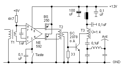
Two BS250 P-channel MOSFETs can be substituted for the 2N3906's if desired. A broadband output transformer in lieu of the parallel tuned circuit is also worth a try. The 10-ohm emitter resistor, capacitor C1 and the 10 uH choke all disappear if FETS are employed. This design probably represents an all-time low in parts count to achieve 1 watt of linear power output, with only 8 components. Note, however, that the 2N3906's actually produce 50% more output for very little added complexity. We could stop at this point, connecting our 1-watt powerhouse to an antenna (via a low pass filter, of course!), or use this circuit to drive an a RF power transistor of more substantial proportions, as shown below. Depending on the frequency, we can achieve 4 to 6 watts output with 0,5 to 0,75 amps current consumption from our 13.8 VDC supply, using a Japanese bipolar device (2SC2078) intended for CB radio and similar applications.
Fig. 2: MOSFET's and RF power transistor
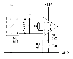
The NE592 differential input has a relatively high input impedance and is therefore suited for direct coupling via an L/C parallel resonant circuit tuned to the transmit frequency. An input impedance of 1 K-ohms results in a stage gain of 100. A lower resistance can increase the gain, but at the expense of input impedance, loading down the input tank. The output circuit, to the right of the NE592 is similar to figure 1 or 2.
Fig. 3: Connection to the NE612 mixer
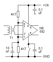
A variant for input control at high frequency is shown in the following drawing. Here the RF at the base of the first transistors inside the NE592 is grounded and the input signal is fed symmetrically to both emitters. One or two secondary turns on the broadband transformer T1 are sufficient due to the low input impedance of a common base configuration. 1,5 W at 24 MHz and 13,8 V supply voltage are generated by this circuit together with the push-pull amplifier out of figure 1. The efficiency is about 70 %.
Fig. 4: Control with common base configuration
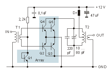
Push-pull Final with a Transistor Array
One can build in an easy way a small push-pull amplifier with the five transistors of the CA3083 array and some passive components. For more power two times two transistors (Q2 +Q3, Q4 + Q5) are working in parallel. Normally used emitter resistors for balancing the collector current are missing here, because all transistors in the array have identical parameters. The lack of this resistors affects itself positively to the efficiency. Q1 is used as a diode and it takes over the bias adjustment. It has a perfect thermal coupling to the other four final transistors due to the integration in the same case.
During the unavoidable rise in temperature in operation the bias voltage is reduced accordingly and thus collector current runaway is prevented. The quiescent current through Q2... Q5 should amount in total 25 mA. It can be adjusted to this value by a resistance different to 2,2 KOhm, if necessary. The final produces an optical clean sine wave due to the AB biasing and the tank circuit tuned to 7 MHz. At 12 V supply voltage and a 200 mA current consumption the stage outputs approx. 1.5 watts of RF energy at 50 ohms . T1 is a FT37-43 ferrite core with 3 x 3 turns (trifilar) and T2 a T44-2 iron core with 3 x 8 turns (trifilar). For Dr a VHF choke with a 6-hole core was used.
Fig. 1: Schematic of the push-pull final
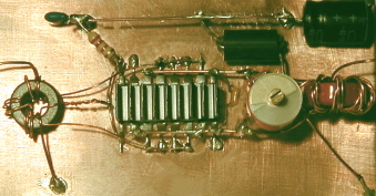
The following photo shows a "dead bug" construction on a small piece of unused PC board. The array is laying with its lower surface directly on the board. For this mounting method one must high-bend up first all pins carefully in the full length by 90°. Now coat some heat-sink compound on the array, place it on the copper layer, bend all emitter pins downward and solder them. This mounting causes a perfect ground connection and excellent cooling of the array. Who still something property wants to do can additionally set a small finned heat sink on the array.
Fig. 2: "Dead bug" construction
Attempts with more driving power and 13,8 V supply voltage resulted in 2,7 watt output power. But operation with this performance is not recommended with respect to the amplifier reliability. The transistors operate on their power limit. Further the linearity worsened starting from 1,5 watts due to the over-proportionally increasing driving power.