Many thanks to Andreas DJ3EI for the excellent revision of the following text
GM47: Simple 30m Band QRP CW-Transceiver
This simple QRP transceiver for the 30 m band did not result from a detailed requirement profile. I simply had some NE592 broadband amplifiers in my junk box, waiting for an application. After performing some tests, that application was quickly found: The amps should become part of a superhet transceiver. There is need for amplification in several places in such a rig, starting from the IF, over to the AF, and up to the RF for driving a push-pull final.
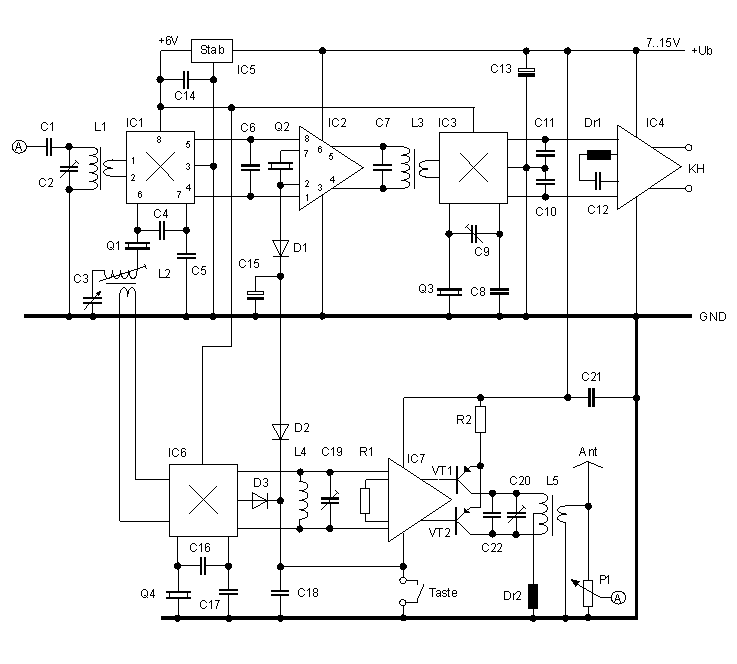
Fig.1: Transceiver schematic
Variable crystal oscillator VXO
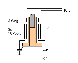
The high crystal frequency of 14318 kHz allows a pulling range of 20 kHz without special tricks. You can tune the reception range from 10100 kHz to 10120 kHz using the coil L2. Some tests with the number of turns of the coil are recommended here, such tests are commonplace when setting up a VXO.
The oscillator signal is coupled into the transmitter mixer through a small link winding on L2, so the Tx mixer can be driven symmetrically. I first tried a capacitive connection, for example 10 pF at pin 7 of IC 1, but found that too much of the rig's own radiated RF got picked up that way.
Fig. 2: Detailed view of L2
Rx mixer and IF amplifier
The Rx mixer is followed by a IF stage featuring an NE592. The mixer's balanced output is directly connected to the amplifier's differential input, minimizing component count at this point. I got a sufficiently narrow bandpass action for the selection of the intermediate frequency using a single 4194 kHz crystal as the only Z element.
Product detector and AF amplifier
The second mixer operates as a product detector. It is followed by a NE592-based selective audio amplifier. The RF portion of the mixer's output signal is surpressed by the two capacitors C10/C11. The remaining AF signal is directly fed into the differential input of the NE592.
The AF stage's frequency response is determined by the series resonant circuit DR1/C12. The stage has a gain of 42 dB at a measured center frequency 660 Hz. The volume adjustment takes place with the RF attenuator P1 close to the antenna input.
Headphones with an impedance of at least 1 kOhm are mandatory here, due to the relatively high output impedance of the NE592. A LM386 is actually the preferential component for driving headphones, or a 8 ohms loudspeaker. But I wanted to try something different this time.
Tx mixer, driver and power amplifier
A NE592 does its job also here. Due to its relatively high input impedance, it can be attached directly to the parallel resonant circuit L4/C19. Its 8 mW power output of the broadband amp is sufficient to drive a small push-pull transistor stage.
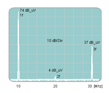
One pair of PNP transistors 2N3906, together with the tuned tank circuit C20/C22/L5, produce an optically clean sine wave. A measurement of the output spectrum showed the second harmonic to be down -70 dB and the third -37 dB, when compared to the power output at the fundamental frequency. The maximum power output is about 1.5 W when the unit is supplied with Ub=13.8 V.
Fig. 3: Measured output spectrum
Rx/Tx control
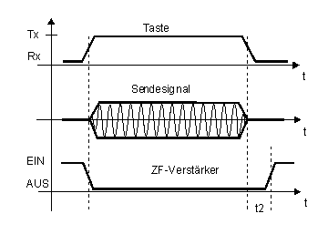
During transmit, the IF stage is muted with two schottky diodes D1 and D2. Pulling the emitter of the first transistor pair inside the NE592 against ground via pin 2 looks somewhat brutal, but it works. The receiver is almost deaf and only the own transmit signal is audible as a side tone in the background.
The delayed starting of the crystal oscillator Q4, and hence the delayed generation of the transmit signal, reduces the intensity of on-clicks. A change from transmit to receive disables the transmit stage by disconnecting the Tx mixer and driver from ground potential. The IF stage becomes operational some delay t2 later, after C15 has been charged through IC2 and D1. This delay reduces the audibility of switch-off clicks to a tolerable level.
This Rx/Tx control circuit has been found sufficent for a medium keying speed, but requires a low key on resistance. When connecting an electronic key to this rig, a 0.47 µF capacitor between pin 1 of IC6 and the cathode of D3 noticeably improves the switch-on behavior.
Fig. 4: Rx/Tx timing
Power supply
The transceiver operates in a power supply voltage range of Ub=8 ... 15 V. All broadband amps are supplied with Ub, while IC5 provides all mixers with a stabilized 6 V voltage. Diode D3 ensures that the voltage at pin 3 of IC7 can rise up to +Ub during receive mode, without causing harm to IC6. IC7 is then without supply voltage and therefore generates no additional noise.
The transceiver consumes 40 mA during receive and up to 180 mA during transmit. You can reduce the rig's current hunger by 20 mA if you replace the AF amplifier IC4 with a dual op amp, e.g., of the type TL072/082 (see chapter "selective audio amplifier"), and by using a 6 V regulator IC5 with low quiescent current.
Construction
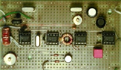
Two strip-board PCB's with dimensions 5 cm x 10 cm were used for the initial construction. The placement of the components on these boards was nearly identical to the one in the schematic. I think, a layout design, e.g., with Eagle light shareware version, or with a graphical editor, should be a relatively straightforward matter.
Fig. 5: Initial construction
 |
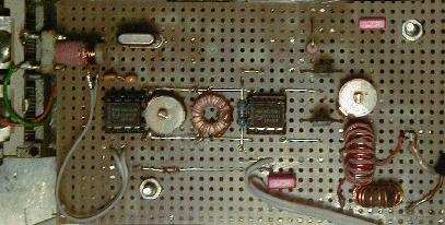 |
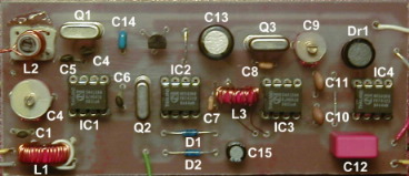
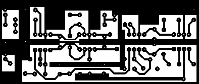
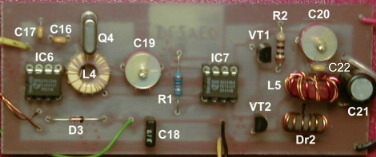
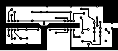
Meanwhile, a semi-professional layout is ready. Here's one picture of the component side and one of the soldering side. This PCB layout is not optimized for minimal space. The target was a simple arrangement, leaving sufficient distance between components.
Fig. 6: PCB layout and assembly
| Receiver | ||
 |
 |
|
| Transmitter | ||
 |
 |
Alignment
To align the transceiver, an existing main-station rig and an oscilloscope are sufficient. First tune the VXO frequency with L2 to 14.294 kHz (C3 max.) and 14.314 kHz (C3 min.). Now tune the input resonant circuit with C2 to 10110 kHz; i.e., max. volume of an amateur radio station working on this frequency. C9 determines the BFO frequency offset and thus the pitch of the AF signal. For maximum AF output level, the frequency offset of the BFO should correspond with the resonant frequency from C12/DR1.
Next, the two trimmer capacitors in the transmitter section are adjusted, first C19 and then C20, on best sine wave and maximum output power, respectively. With a supply voltage of Ub=13.8 V, approximately 25 Vss should be delivered to a 50 ohm dummy. Subsequently, check the the value with an adapted antenna. However, the signal may look somewhat noisy, due to superimposed received signals getting in from the antenna.
Parts list
You can get all electrical and mechanical components for less than $35. You could possibly encounter some difficulties purchasing variable broadcast capacitors and high impedance headphones. But a review of the junk box of a friendly OM, a visit to a ham radio flea market, or stripping an old radio should solve this problem.
| Parts No. | Value |
|---|---|
| R1 | 1 kOhm |
| R2 | 10 Ohm |
| P1 | 2,2 kOhm , linear |
| C1 | 3,3 pF |
| C2, 9, 19, 20 | 5 .. 90 pF trimmer cap |
| C3 | 20 ... 320 pF variable broadcast capacitor |
| C4, 5, 6 | 56 pF |
| C7 | 330 pF |
| C8, 17, 22 | 220 pF |
| C10, 11 | 1,8 nF |
| C12 | 2,2 µF |
| C13 | 100 µF, 25 V |
| C14, 18, 21 | 0,1 µF |
| C15 | 47 µF, 16 V |
| C16 | 100 pF |
| L1 | T50-2, 30 t primary 3 t secondary |
| L2 | Diameter=4 mm, Hight=12 mm, approx. 2 x 16 t and 3 t (RF pick up) |
| L3 | T37-6, 35 t primary 5 t secondary |
| L4 | T37-6, 35 t |
| L5 | T44-2, 5 t bifilar primary 5 t secondary |
| Dr1 | 33 mH |
| Dr2 | FT37-43, 16 t |
| Q1 | 14318 kHz |
| Q2, 3, 4 | 4194,3 kHz |
| D1, 2 | BAT 42 |
| D3 | 1N4148 |
| VT1, 2 | 2N3906 with a small heat sink |
| IC1, 3, 6 | NE612 DIP |
| IC2, 4, 7 | NE592-N8 DIP |
| IC5 | 78L06 |
| KH | Headphones Ri > 1 kOhm |
Closing Remarks
As there is enough gain available in the IF stage, this design can deviate from conventional QRP schemes by using a very lightly coupled tuned parallel resonant circuit with high Q ahead of the Rx mixer. The resulting preselection, the narrow bandwidth IF filter,