Many thanks to David Ai2A for the excellent revision of the following text
40 m Band Direct Conversion Receiver
Building a practical and usable direct conversion receiver for the 40 m CW band is not as simple as it might appear. Broadcast station signals from the adjacent 41 m band, will easily overload most direct conversion mixer designs with their unwanted (and quite nearby) S9 +40 dB signals. My solution incorporates a diode-ring mixer and a narrow band rf input filter. These choices result in observed overall receiver dynamic range than that experienced when using an IC mixer module (such as a NE612). Comfortable and undisturbed operation in the evening was possible when tested using my Windom antenna. Some of this project's objectives included:
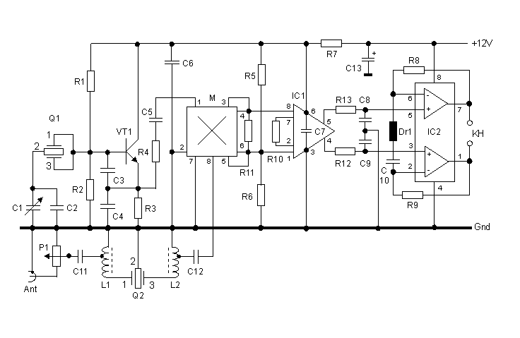
You may recognize many of the stage circuits - as they are similar to those used in some of my other projects. The VFO and the RF input band pass filter are each designed around ceramic resonators. These are becoming difficult to locate. [See the note below.] I have used a HPF505 type ring diode mixer - but other mixers such as the IE500 or SRA1 should be suitable. The diode ring mixer output drives a parallel arrangement consisting of R11 and the differential input impedances of IC1. This results in a more stable 50-Ohm broadband termination for the mixer output (by contrast to that possible on a typical RCL based diplexer).
The gain of the broadband amplifier following the mixer, IC1, is set by the choice of R10. A 40 dB gain is achieved by using 100-Ohm resistor at R10. Any IC1 rf output signals are shunted to ground - leaving only an audio signal to be applied to the following stage. IC2 is an operational amplifier that is used to amplify the remaining audio signals by yet an additional 46 dB. Passive audio filter components are used at the input of IC2 so that only signals at or near 750 Hz are amplified. The overall gain and output level is almost too great for comfortable headphone listening. An rf attenuator (P1 located near the antenna input terminal) is used as a means of controlling the receiver output volume
Fig.1: Receiver schematic
Perhaps the most critical objective in this design is the voltage present at Pin 6 of IC1 (broadband amplifier). Adjust the value of R7 slightly as needed to set the voltage at IC1 pin 6 to be very close to +8 V. IC1 (at its output pins 4 and 5) provides the dc bias voltage of +6 V (Ub/2) as required for the non-inverting opamp inputs of the final amplifier stage, IC2. The dc input bias for this circuit is relatively critical if distortion is to be minimized. This opamp circuit can provide an undistorted audio output (at pins 1 and 7 of IC2) of as much as 10 Vss. When properly built and adjusted, this receiver should consume only about 25 mA with the antenna disconnected. The receiver functions well at any power supply voltage ranging from +15 V down to as low as +9 V.
| Parts No. | Value |
|---|---|
| R1 | 27 kOhm |
| R2 | 22 kOhm |
| R3 | 470 Ohm |
| R4 | 330 Ohm |
| R5,6 | 4,7 kOhm |
| R7 | 220 Ohm |
| R8,9 | 10 kOhm |
| R10 | 100 Ohm |
| R11 | 51 Ohm |
| R12,13 | 1 kOhm |
| P1 | 1 kOhm, linear |
| C1 | 20 ... 325 pF, variable capacitor |
| C2 | 100 pF |
| C3 | 680 pF |
| C4 | 330 pF |
| C5,11,12 | 4,7 nF |
| C6,7 | 0,1 µF |
| C8,9 | 47 nF |
| C10 | 2,2 uF, no electrolytice cap |
| C13 | 100 uF, 25 V electrolytic cap |
| Dr1 | 33 mH |
| L1,2 | FT37-43, 5 turns tap at the second turn |
| Q1,2 | SFE 7.02 M2C, Murata |
| VT1 | 2N3904 |
| IC1 | NE592-N8 DIP |
| IC2 | NE5532 DIP, dual opamp |
| M | Mixer HPF505, IE500, SRA1 e.g. |
| KH | Headpho |