Many thanks to James G3RUH for the excellent revision of the following text
HPF-505, SRA-1, SBL-1, IE-500: Mixer
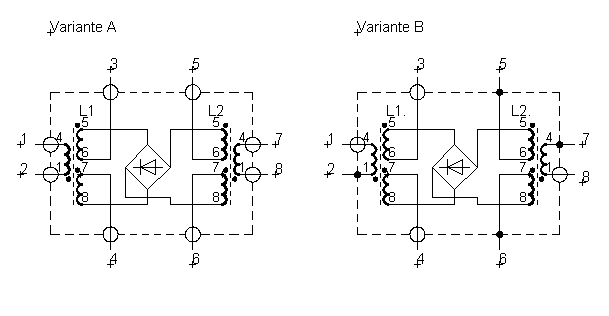
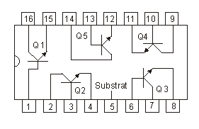
Fig.1 below shows the internal circuitry of well known mixers IE-500, SRA-1, SBL-1, HPF-500 and others. An empty circle stands for an isolated service through the mixer case, whilst a small filled dot indicates the pin is electrically connected to the case. Usually those pins are at ground potential, GND.
Fig. 1: Internal circuitry and meaning of pins
Typical usage of ports:
| Pins | Variant A | Variant B | Toroid | Internal connection |
|---|---|---|---|---|
| 1 | RF Port | RF Port | L1 | (4) |
| 2 | GND | L1 | (1) | |
| 3+4 | IF Port | IF Port | L1 | (6) and (7) |
| 5+6 | GND | L2 | (6) and (7) | |
| 7 | LO Port | GND | L2 | (4) |
| 8 | LO Port | L2 | (1) |
Pin 1 is colour coded BLUE or marked specially. LO Port and RF Port are identical in their function and can be exchanged if required. Only variant A allows for symmetrically driven ports and isolated IF signal. With variant B all ports are single-sided connected to the case thus to ground GND. For proper mixer operation of variant A, pins 3/4 and 5/6 have to be linked together externally.
Fig. 2: Variant A, bottom view
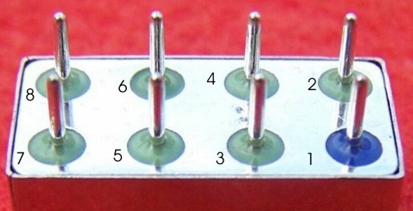
Fig 3: Variant A, internal
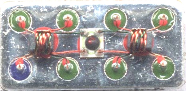
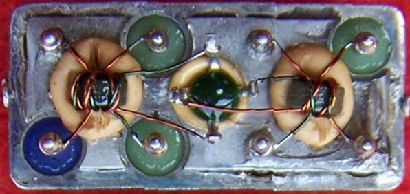
The HPF-505 seems to be available in both variants. I got variant A when I bought one. From there I was able to realize the symmetrical connection to an AF and IF stage, as shown by the superhet RX and direct conversion RX. At that time I did not know that variant B of HPF-505 existed. A representative of this group is the HPF-505X-1 from Mini-Circuits. In the picture one can clearly see the electrical connection of pins 2, 5, 6 and 7 directly to the case.
Fig 4: Variant B, e.g. HPF-505X-1
NE592: Broadband Amplifier
This broadband amp is intended as a video amplifier. It has a maximum gain of 400 (52 dB) and unity bandwidth of 120 MHz. Noticeable gain reduction begins at f > 20 MHz. Differential inputs and outputs are further features of this op amp. Gain and frequency responses can be influenced over a wide range by means of a Z network between pin 2 and pin 7.
Fig. 1: Broadband amplifier NE592
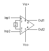
Test circuits show that this component can self-oscillate depending on Z elements' placement, output loading, bias adjustment and so on. Parasitic capacitance in parallel to the Z elements and inside the op amp lead to undesired amplification of high frequencies. For an AF application no RF energy is allowed at the differential inputs and for RF application the capacity becomes part of the Z network design. Compared with the 14 pin IC, the 8 pin version has no G2A and G2B terminal for fixed gain adjustment.
Fig. 2: Internal circuit
When placing the Z elements on the board, take care that they are located on the same side as the input pins. Placement close to the output pins often leads to self oscillation. Elements that are fixed directly below the IC package can sometimes give an improvement in critical applications. Short leads and a good ground plane are mandatory.
Tab.1: Absolute limits
| Symbol | Parameter | Value | Unit |
|---|---|---|---|
| Vcc | Supply voltage | +/- 8 | V |
| Vin | Differential input voltage | +/- 5 | V |
| Vcm | Common mode voltage | +/- 6 | V |
| Iout | Output current | 10 | mA |
| Ta | Operating temperature | 0 ... 70 | °C |
DC data at Tu=25°C, VSS=+/-6 V and Vcm=0 V:
| Symbol | Parameter | Test condition | Value | Unit |
|---|---|---|---|---|
| Avol | Differential gain | Rl=2 kOhm, Vout=3 Vss | 400 | V/V |
| Rin | Input resistance at different gain adjustments by Radj | Radj=1 Ohm | 4 | kOhm |
| Radj=100 Ohm | 30 | |||
| Vout | Differential output voltage | Rl=2 kOhm | 4 | Vss |
| Icc | Supply current | Rl >> | 18 | mA |
A big advantage is that this broadband amplifier can be easily purchased. It costs less than 50 cents depending on the supplier. So during experimentation destroyed amps aren't an issue. The amp is also listed in parts catalogues (e.g. Reichelt) as SA592. You can download a detailed data sheet from the Philips-Semiconductors-Homepage.
NE612: Mixer and Oscillator
You'll see the NE612 in homebrew projects very often. Functionally compatible with this type are the SA612/NE602 as well as the SA602. The 8 pin package contains a double balanced mixer (Gilbert cell), input biasing, a buffer and a separate transistor usable as an oscillator. With a minimum of three additional passive components one can build a Rx/Tx mixer including VFO/VXO, or a product detector with BFO. Remember that the large signal behaviour of the mixer is very modest compared to a ring diode mixer. In applications such as a RX mixer, good pre-selection is strongly recommended. Intermodulation appears, particularly in the evening hours, if strong signals from broadcast stations - hardly or not sufficiently attenuated - reach the mixer inputs.
Fig. 1: Internal Circuit
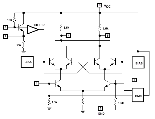
Detailed technical data can be taken from the data sheet NE612 of PHILIPS. Examples for the oscillator design and the input/output circuitry are described in the AN1982 and AN1983 application reports.
Tab.1: Technical data
| Symbol | Parameter | Value | Unit |
|---|---|---|---|
| Vcc | Supply voltage | 4,5 ... 8,0 | V |
| Icc | Supply current | 2,4 ... 3,0 | mA |
| Rin | RF input resistance (Pin 1/2 against GND) | 1,5 | kOhm |
| Rout | Mixer output resistance (Pin 4/5 against GND) | 1,5 | kOhm |
| Mixer gain | 14 ... 17 | dB | |
| IP3 at RFin=-45 dBm | -13 | dBm | |
| fosc | maximum oscillator frequency | 200 | MHz |
| fmix | maximum mixer frequency | 500 | MHz |
| Signal to Pin 6 by an external iscillator | 200 | mV |
Take into consideration twice the resistance (2 x 1,5 kohm) with symmetrical use of inputs and outputs.
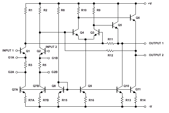
Component: CA3083 transistor array
This 16 pin transistor array contains five 100 mA NPN transistors. They have identical parameters due to integration on a common substrate. Its advantage is universal use; every transistor terminal is accessible.
Fig. 1: Internal circuit
The transistor array can be readily purchased and costs less than 50 cents depending on the supplier. You can download a detailed CA3083 data sheet from the Intersil Homepage.
Tab.1: Absolute limits
| Symbol | Parameter | Value | Unit |
|---|---|---|---|
| VCE0 | Collector-to-Emitter voltage | 15 | V |
| VCB0 | Collector-to-Base voltage | 20 | V |
| VEB0 | Emitter-to-Base voltage | 5 | V |
| IC | Collector current | 100 | mA |
| IB | Base current | 20 | mA |
| P | Power dissipation (any one transistor) | 500 | mW |
Tab.2: Electrical specification at TA=25°C
| Symbol | Parameter | Test condition | Value | Unit |
|---|---|---|---|---|
| VCEsat | Collector-to-Emitter saturation voltage | IC=50 mA, IB=5 mA | 0,7 | V |
| hFE | DC Forward-Current transfer ratio | VCE=3 V, Ic=50 mA | 75 | - |
| f |