Many thanks to David Ai2A for the excellent revision of the following text
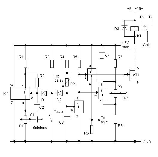
Tx/Rx Control Circuit
This circuitry offers some features that are highly desirable when building a QRP (or ANY) transceiver. It also includes a combination of features that many might not always take the time to include in their projects. Considerable effort has been made to assure that in this design, the RIT (RX frequency offset control) voltage and the TX frequency offset control signals are immune to supply voltage variations. IC1 requires a regulated +6 V voltage for proper operation. This is achieved by using the highly regulated VFO power supply rail. The main power supply rail (+9 to +15 V unregulated) powers the relay coil and its transistor circuit. The separate power sources improves the stability. Some features included in this control circuit include:
When the key is pressed down, the antenna relay coil needs to be quickly energized. One of the sections within IC1 is assigned this task. The voltage on pin 13 determines if the output at pin 1 is at a logic high or low level. Since C3 is quickly discharged via a blocking diode, D2, when the key is pressed, IC1 pin 1 is set to a high output logic level. This level biases the VT1 into conduction, enabling relay coil current flow. When energized, K1 switches the antenna from the receiver input to the output of the TX.
To understand how this works, observe that voltage is applied to C3 via the variable resistance of control P2. This forms an RC timebase circuit. When a voltage is applied via the resistance of P2, energy will be stored in C3. As the amount of energy stored in C3 increases - the voltage measured across C3 will also rise. As this voltage steadily rises to a level beyond the threshold needed by IC1 pin 13, the output from IC1 pin 1 will revert back to its logic Low-level. Bear in mind that so long as the key is pressed, the voltage from P2 is shunted to ground and thus does not store a charge in C3.
When the key contact is opened, C3 will begin to build up a charge via P2 and R4 since it is no longer being shunted to ground. As time elapses, the voltage across C3 rises to the threshold level, allowing IC1 pin 1 output to return to its Logic low resting state. When this occurs, it will lower the bias voltage seen at the gate on VT1's Drain to Source current will stop thus relay coil current will cease. Without relay current, the relay reverts back to its unenergized state (receive). By altering the setting of P2, the break-in delay can be altered to any desired break-in delay between 100 ms to 5 sec. Be sure that you include diode D3 since it clamps any reverse-emf developed across the relay coil as the magnetic field collapses. Such reverse-emf is sufficient to destroy the transistor VT1.
Fig.1: Tx/Rx control
As long as this circuit is in the receive mode one can adjust the VFO frequency with P3 a little - forming the RIT feature. This works by offering a bias voltage, which can be applied to a varactor diode in the VFO. This voltage can range anywhere from +1 to +5 V. In practice, this control P3 should be set to the center of its range so the RIT can be varied either above to below the desired frequency. The RIT voltage is switched to a constant +3 V at P3 - during transmit. A 700 Hz timebase circuit is formed by fixed resistor R2 and fixed capacitor C2. So long as the key is pressed, the C2 is going to be charged and discharged in at a 700 Hz cycle rate via R2. When the key is not pressed, IC1 Pin 6 input is immediately forced high via resistor R3 and diode D1 preventing to 700 Hz switching activity. Sidetone output volume level can be set with P1.
It may be desirable to provide the transmitter with a voltage capable of shifting the VFO by 700 Hz. This provides a +6 V during transmit for VFO varactor bias at IC1 pin 4. If the opposite is desired (i.e. 0 V at Tx and +6 V at Rx):
A superhet does not generally require the Tx shift signal. The BFO is generally set to a point about 700 Hz from the received carrier. In such a case, the third CMOS switch (pins 3, 4, 5) can be used for any other desired activity - such as muting of a Receiver AF stage.
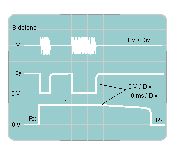
Fig.2: Control signals over the time axis
A pair of resistance networks can be used as described here. A network puts multiple resistors in a single very compact package. This construction is more compact compared to using discrete resistors. The first network contains five resistors with a common terminal and the second network has three resistors without any common terminals..
| Parts No. | Value |
|---|---|
| R1,3,4,5,7 | resistance network 5 x 10 kOhm, 6 pins |
| R2,6,8 | resistance network 3 x 10 kOhm, 6 pins |
| P1 | 5 kOhm, linear |
| P2 | 500 kOhm, linear |
| P3 | 100 kOhm, linear |
| C1 | 4,7 nF |
| C2 | 0,1 uF |
| C3 | 2,2 uF |
| C4 | 47 uF, electrolytic cap. |
| D1,2,3 | 1N4148 |
| VT1 | BS170 |
| IC1 | 4066B, quad CMOS switch |
| K1 | 12 V miniature print relay, R_coil |