I would be grateful for a professional translation or correction of the following text. Please E-Mail to Delta Lima 2 Yankie Echo Oscar @ Queen Romeo Papa 4 Uniform .Delta Echo
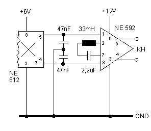
AF Amplifier based on NE592
The broadband amplifier NE592 can be used also for building a simple selective audio amplifier. By means of the +6 V and +12 V supply voltages a DC coupling between the product detector and the AF amplifier is possible. The DC level at the differential inputs is about 4,5 V. The mixer drives the differential input of the NE592 - after suppression of the RF proportions by two 47 nF capacitors - with the remaining AF signal. RF blocking between the outputs is feasible with only one capacitor, but not between the single outputs and ground. But the latter is absolutly necessary due to the wide amplifier bandwidth. The AF stage offers a gain of 200 (46 dB) at 660 Hz center frequency
Fig. 1: AF amplifier with NE592
Headphones with Ri > 1 kOhm are mandatory due to the relatively high output resistance of the NE592 amp. 18 mA quietscent current isn't low, but it is insignificant in case of stationary operation and supply by a small ac-operated power supply.
Fig . 2: Transfer characteristic
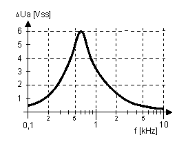
The selectivity isn't excelent, but better than none. Usual CW audio filters with e.g. four op amps need many times more components.
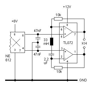
AF Amplifier based on TL072
You can reduce the AF stage current consumtion down to 2 mA when with a dual op amp TL072/082 instead of the NE592 broadband amp. These consumer op amps have a lower output resistance, so that they are able to drive 2 x 32 ohms headphones connected in series with a 470 ohms resistor. When using a NE5532 no additional resistor is necessary, because the outputs have a less lower impedance. The transfer characteristic is the same as the one displayed for the first circuit (AF amp with NE592)
Fig. 1: AF amplifier with a dual op amp TL072
AF Amplifier based on 2N3906/3904
Low distortion, CW selectivity, high gain, low noise and a high output
voltage are the features of the following circuit. This circuit is seldom used
despite its good characteristics. The latter is perhaps because of the fact
that one must try different resistance values for R4 and R5 depending upon the
quiescent current through IC1. This is ok for building a single device but not
acceptable for a series product.
Fig. 1: 0,5 W audio amplifier
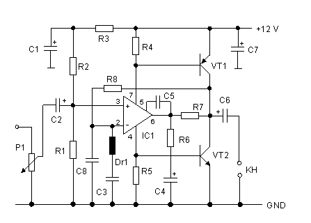
For low distortion an perfect bias adjustment of the transistors VT1/2 is
necessary. One must define the resistance value of R4 and R5 in such a way that
VT1 and VT2 get a base emitter voltage of approx. 500 mV dc with no drive
signal. The series resonant circuit Dr1 and C3 is responsible for the CW
selectivity. In case of resonance the stage has a gain of V = (1 -
R8 / Rres) = 60. The frequency transfer characteristic is identical
to the one of the first circuit (AF amplifier based on NE592).
Fig. 2: Output signal
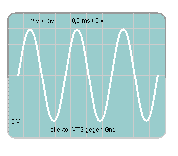
Contrary to the usual complementary stages with a common-collector
arrangement, the output voltage attainable with this principle is almost equal
the operating voltage (12 V - 2 x Uce). The good value acquires one with an
increased output resistance, which is caused by the transistors operating in a
common-emitter arrangement. The output resistance is optimal for headphones
that have an impedance between 32 and 64 ohms. The current consumption (5 to 50
mA) depends upon the drive level and the load resistance.
| Parts | Value |
|---|---|
| R1 | 10 kOhm |
| R2 | 8,2 kOhm |
| R3 | 1,8 kOhm |
| R4, 5 | 390 Ohm |
| R6 | 47 Ohm |
| R7 | 470 Ohm |
| R8 | 4,7 kOhm |
| C1,4 | 47 uF, electrolytic cap. |
| C2 | 10 uF |
| C3 | 2,2 uF |
| C5 | 150 pF |
| C6,7 | 100 uF, electrolytic cap. |
| C8 | 220 pF |
| P1 | 10 kOhm, linear |
| Dr1 | 33 mH |
| VT1 | 2N3906 |
| VT2 | 2N3904 |
| IC1 |